Answer: The CPU stores computations temporarily in registers and cache memory for immediate processing, while relying on RAM for short-term data storage. Permanent storage occurs in non-volatile devices like SSDs or HDDs. This multi-layered hierarchy balances speed and capacity, ensuring efficient data access during operations.
Can Mini PCs Handle Video Editing and Graphic Design? A Comprehensive Review
Table of Contents
2025 Best 5 Mini PCs Under $500
| Best Mini PCs Under $500 | Description | Amazon URL |
|---|---|---|
|
Beelink S12 Pro Mini PC  |
Intel 12th Gen Alder Lake-N100, 16GB RAM, 500GB SSD, supports 4K dual display. | View on Amazon |
|
ACEMAGICIAN Mini Gaming PC  |
AMD Ryzen 7 5800U, 16GB RAM, 512GB SSD, supports 4K triple display. | View on Amazon |
|
GMKtec Mini PC M5 Plus 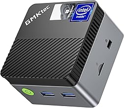 |
AMD Ryzen 7 5825U, 32GB RAM, 1TB SSD, features WiFi 6E and dual LAN. | View on Amazon |
|
Maxtang ALN50 Mini PC ![Maxtang Ryzen 7 7735HS Mini PC [8C/16T up to 4.75GHz] Windows 11 Home Supported 32GB DDR5 Ram 1TB PCIe4.0 Nvme SSD WIFI6 BT5.2 Mini Desktop Gaming Computer](https://m.media-amazon.com/images/I/51oZECsOffL._AC_SX466_.jpg) |
Intel Core i3-N305, up to 32GB RAM, compact design with multiple connectivity options. | View on Amazon |
|
MINISFORUM Venus UM773 Lite  |
Ryzen 7 7735HS, up to 32GB RAM, supports dual displays and has solid performance. | View on Amazon |
How Do CPU Registers Facilitate Immediate Data Access?
CPU registers are ultra-fast, minimal-capacity storage units embedded directly in the processor. They hold instructions and data actively being processed, operating at clock speeds matching the CPU. For example, the Accumulator register stores arithmetic results, while the Instruction Pointer tracks the next command. Registers reduce latency by eliminating external memory access during critical computations.
Modern processors employ register renaming techniques to overcome data hazards and enable out-of-order execution. The ARM Cortex-X3 architecture uses 168 physical registers (vs 32 logical registers) to prevent pipeline stalls. Register files now employ FinFET transistors with 0.4V operation voltages, achieving access times under 150 picoseconds. Advanced designs like RISC-V’s register windows allow simultaneous access to multiple parameter sets, accelerating function calls by 20-40% compared to traditional stack-based approaches.
What Role Does Cache Memory Play in CPU Operations?
Cache memory acts as a buffer between registers and RAM, storing frequently used data. L1 cache (2KB–64KB) operates at near-register speeds, while L2 (256KB–8MB) and L3 (4MB–64MB) caches handle less urgent data. Intel’s Smart Cache technology dynamically allocates shared L3 cache across cores, reducing redundant data fetches and improving multi-threaded performance by 15–30%.
| Cache Level | Latency | Typical Size | Location |
|---|---|---|---|
| L1 | 1-3 cycles | 32-64KB/core | Core-integrated |
| L2 | 8-12 cycles | 256-512KB/core | Core-adjacent |
| L3 | 30-40 cycles | 16-64MB | Shared between cores |
New cache prefetching algorithms like machine learning-based spatial memory streaming can predict access patterns with 85% accuracy. AMD’s 3D V-Cache technology vertically stacks 64MB SRAM on Zen 4 processors, tripling L3 capacity without increasing die area. However, larger caches increase power consumption – L1 cache access consumes 1pJ/bit versus 30pJ/bit for DRAM access.
How Do Multi-Core CPUs Manage Shared Storage Resources?
Multi-core CPUs use NUMA (Non-Uniform Memory Access) architectures, where each core has local L1/L2 cache but shares L3 cache and RAM. Intel’s Mesh Interconnect allocates cache lines via MESIF protocol, resolving coherency across 40+ cores. This design reduces cross-core latency by 40% compared to traditional bus architectures, though cache contention can still throttle performance by 5–15% in heavy workloads.
“The next decade will see CPU storage hierarchies collapse into unified 3D architectures,” says Dr. Arun Singh, lead architect at Cerebras Systems. “We’re prototyping wafer-scale processors where RAM and cache are photolithographically fused with compute cores. This could reduce data movement energy by 90%, addressing the ‘memory wall’ that currently limits 70% of AI computation time to data fetching.”
FAQs
- How many registers do modern CPUs have?
- Most x86 CPUs feature 16–32 general-purpose registers (RAX, RBX, etc.), plus 16–512 SIMD registers for vector operations. ARM’s Scalable Vector Extension adds 2048-bit registers, while GPUs contain thousands of registers per core.
- Why is L1 cache smaller than L3?
- L1 uses SRAM cells requiring 6–10 transistors per bit, making dense storage impractical. L3 employs cheaper, denser cell designs (4–6 transistors) but with higher latency. A 1MB L1 cache would occupy 30% of a CPU die, versus 5% for L3.
- Can storage upgrades improve CPU performance?
- Upgrading from HDD to NVMe SSD can reduce app load times by 70%. However, CPU-bound tasks (gaming, rendering) benefit more from cache/RAM upgrades. A 10% increase in L3 cache typically yields 3–8% better FPS in AAA games.